Changelog
Version | Date | Author | Summary
-- | -- | -- | -- | --
2.0.1 | 2018-02-22 | Fallberg/Anticimex | Clarification on pin1 orientation.
2.0 | 2016-09-08 | Fallberg/Anticimex | Version 2 released. Specifies MYSX rev. 2.0-2.6.
1.2 | 2015-12-04 | Fallberg/Anticimex | Clarified mother/daughterboard connector types.
1.1 | 2015-08-21 | Fallberg/Anticimex | Clarified pin numbering on the header.
1.0 | 2015-07-18 | Fallberg/Anticimex | Initial version of specification. Specifies MYSX rev. 1.0-1.5.
Abstract
The MySensors expansion connector serves as a uniform interface between official MySensors boards and MySensors (or user created) daughter boards. This document describes hard requirements on the connector (pinouts and required/expected pin capabilities) and soft requirements (placement/layout considerations).
The connector comes in several versions where each new sub-version is backwards compatible with previous versions.
That is, v2.5 will be compatible with 2.3 and 2.0. In other words, every new sub-version will expand on the existing connector capabilities, but never reduce capabilities. It is for this reason also assumed that every board that implement the MYSX connector stick to a revision where it can provide all the features of that particular revision.
Layout/Placement Considerations
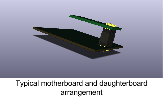
The MYSX connector should be placed close to the board edge with a 100 mil spacing from the top and left relative pin1 to the board edges. The footprint has a courtyard outline to emphasise this. It should be oriented so that pin1 is always closest to the board corner. This allows a daughter board designed using the same constraints to be facing back "inwards" over the motherboard, and to have a known offset to the motherboard edge on the "top" edge (assuming the MYSX connector is placed with pin1 aligned to the top-left corner of the motherboard). This helps keeping the overall board outline the same shape as the motherboard (where applicable). For this reason, component placement on the motherboard should take into account the presence of a daughter board when placing tall components in vicinity to the MYSX connector.
Also note that for a daughterboard, in order to align the pin numbers properly, the MYSX “component” should be placed on top layer, but be soldered on the bottom layer to create a 1-1 mapping between the boards.
Also the "far" edge of the connector (beyond the highest numbered pins) and the area beyond it should if possible be kept free of protruding components in order to accommodate a daughter board that also can mate with later versions of the MYSX connector.
Connector Characteristics
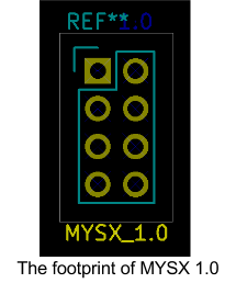
The MYSX connector is a standard 100 mil pitch dual row pin header. The motherboard provides the male part and the daughterboard mates using the corresponding female part.
It is numbered with even numbers in one row and uneven numbers in the other row. The square pad indicate the location of pin 1 and all pins in that row will subsequentally have odd numbers. The connector consists of two (2) rows.
In it’s simplest form, it consists of 8 pins where pins 1-4 are the power rails. The remaining pins are documented in the corresponding revision chapters in incremental order. An optional additional feature of the pin is indicated with parenthesis as are any special considerations for the pin. It cannot be taken for granted that every single implementation of the MYSX connector implement the optional additional pin feature, but if the feature is available on the motherboard, this would indicate where that feature is exported in the connector.
The motherboard board header file provides macros that map the MYSX_ identifiers to the board-specific layout so for any function call involving a MYSX connector signal, the macro should be used. This allows the sketch to be portable across motherboards.
As from MYSX 2.0 it is possible to do FTDI programming through MYSX as both GND/TX/RX, VCC (+3.3V or VCCio depending on MCU board design) and MYSX_RST (MCU reset) is available.
MYSX 2.0
| Pin |
Function |
| 1 |
Vraw (typically unregulated voltage, either from motherboard to daughterboard or vice versa) Motherboard should have a jumper to cut onboard Vraw source if daughterboard provides Vraw. Be sure to check motherboard constraints on Vraw before connecting a daughterboard that provides Vraw (for over voltage protection). Should be able to source at least 100mA and all boards are recommended to support a voltage up to 24V on this pin. |
| 2 |
+3.3V fixed voltage (can source at least 100mA) |
| 3 |
VCCio (depending on MCU core voltage). Should not be used for heavy loads. |
| 4 |
GND |
| 5 |
MYSX_D1_DFM - Digital IO (USART TX (data from MCU)) |
| 6 |
MYSX_D2_DTM - Digital IO (USART RX (data to MCU)) |
| 7 |
MYSX_RST - Reset (On the board that carries the MCU, it is highly recommended that this pin has a 0.1uF capacitor in series for pulse “generation”) |
| 8 |
MYSX_LEGACY_ID – MYSX 1.x identification (2.0 daughterboards can tie this pin to VCC to allow the motherboard to determine if daughterboard is 1.x or 2.x. If identification is not needed or is undesired, pin can be used as regular analog input) |
MYSX 2.1
| Pin |
Function |
| 9 |
MYSX_D3_INT - Digital IO (interrupt) |
| 10 |
MYSX_D4_INT - Digital IO (interrupt) |
MYSX 2.2
| Pin |
Function |
| 11 |
MYSX_D5_PWM - Digital IO (PWM) |
| 12 |
MYSX_D6_PWM - Digital IO (PWM) |
MYSX 2.3
| Pin |
Function |
| 13 |
MYSX_D7_SCL - Digital IO (I2C SCL) |
| 14 |
MYSX_D8_SDA - Digital IO (I2C SDA) |
MYSX 2.4
| Pin |
Function |
| 15 |
MYSX_D9_A3 - Digital IO (analog input) |
| 16 |
MYSX_D10_A4 - Digital IO (analog input) |
MYSX 2.5
| Pin |
Function |
| 17 |
MYSX_D11_MOSI - Digital IO (SPI MOSI) |
| 18 |
MYSX_D12_MISO - Digital IO (SPI MISO) |
| 19 |
MYSX_D13_SCK - Digital IO (SPI SCK) |
| 20 |
MYSX_D14_CS - Digital IO (also for SPI CS) |
MYSX 2.6
| Pin |
Function |
| 21 |
MYSX_A5 - Analog input |
| 22 |
MYSX_A6 - Analog input |
MYSX 1.0
Not recommended for new designs
| Pin |
Function |
| 5 |
MYSX_D1_DFM - Digital IO (USART TX (data from MCU)) |
| 6 |
MYSX_D2_DTM - Digital IO (USART RX (data to MCU)) |
| 7 |
MYSX_A1 - Analog input |
| 8 |
MYSX_A2 - Analog input |
MYSX 1.1
Not recommended for new designs
| Pin |
Function |
| 9 |
MYSX_D3_INT - Digital IO (interrupt) |
| 10 |
MYSX_D4_INT - Digital IO (interrupt) |
MYSX 1.2
Not recommended for new designs
| Pin |
Function |
| 11 |
MYSX_D5_PWM - Digital IO (PWM) |
| 12 |
MYSX_D6_PWM - Digital IO (PWM) |
MYSX 1.3
Not recommended for new designs
| Pin |
Function |
| 13 |
MYSX_D7_SCL - Digital IO (I2C SCL) |
| 14 |
MYSX_D8_SDA - Digital IO (I2C SDA) |
MYSX 1.4
Not recommended for new designs
| Pin |
Function |
| 15 |
MYSX_D9_A3 - Digital IO (analog input) |
| 16 |
MYSX_D10_A4 - Digital IO (analog input) |
MYSX 1.5
Not recommended for new designs
| Pin |
Function |
| 17 |
MYSX_D11_MOSI - Digital IO (SPI MOSI) |
| 18 |
MYSX_D12_MISO - Digital IO (SPI MISO) |
| 19 |
MYSX_D13_SCK - Digital IO (SPI SCK) |
| 20 |
MYSX_D14_CS - Digital IO (also for SPI CS) |