CAUTION: This project deals with hazardous voltage with the risk of death or personal injury! Please don't do anything unless you are absolutely sure of what you are doing. There is no one liable for the correctness or usage of any information below.
Work In Progress
Discussion, work and various projects have been done or are still going on regarding powering our MySensor/Arduino projects from mains supply. So I think the interest in these projects are pretty high. For this reason I decided to share this project as "work in progress" even though I prefer more completeness before publishing. The prototype PCB needs a couple of minor modifications to work. I only share Kicad design files without Gerbers to make sure anyone doesn't order it without being aware of the necessary mods.
The Project Concept
Yet another outlet switch? Well, yes, maybe. Hopefully you'll think I've added some value to it...
I think everyone have seen the cheap remote controlled wireless power outlet switches (here in Sweden usually at 433MHz). They're found in every store. Some are very simple with just a remote control and unknown protocol. Some are rather compatible and then makes quite good as e.g. entry level HA system or part of system. I think most DIY HA system controllers also have the ability to control those protocols and there's also sniffers, bridges and whatever necessary. Here are some threads I found just by a quick search here at the forum:
http://forum.mysensors.org/topic/2286/experimenting-with-cheap-433mhz-gadgets
http://forum.mysensors.org/topic/1621/mysensors-and-433-mhz
http://forum.mysensors.org/topic/1543/universal-gateway-for-315-433mhz-devices
http://forum.mysensors.org/topic/944/one-way-on-how-to-reuse-433mhz-alarming-sensors-for-mysensors
What I dislike most about these simple wireless switches are: (1) No duplx (ack) ability. (2) Unreliable reception. (3) They could interfere with each other if too close. (4) No Atmega328p - no playing. (The more I think about it, the more important is the last (4).)
What I do like most: (1) Cheap (2) Good range. (3) Low power. (4). Small size.
My first idea was to reuse as much as possible and MySensorize one of these common commercial wall-plugs. I did a few tries reusing some parts of the hardware (PCB and power supply) and squeeze in an Arduino Pro Mini and nRF24L01. I failed. The available power wasn't enough because of the relay and when I upgraded the transformerless supply it became to big to fit in the original enclosure. Thus, I looked for a switching transformer supply instead.
Transformerless supplies are great for low power class II devices like this since they're completely insulated. A transformer (-based switch mode-) supply is better for class III devices where the secondary voltage is touchable. But, in this case I had to go for transformer supply because of the space. I can see disadvantages with this choice; (1) Safety - It's much more complex and when ordering from China I'd prefer to trust a single X-cap rather than a whole power supply assembly. (2) Cost - (Not really, because it isn't as great difference as it used to be. Especially considering the work effort with more components of you build a transformerless supply from scratch.).
To make it easy to design and useful for other future projects as well, I looked for a smaller switched mode power supply (SMPS) than the famous HLK-PM01 and then I had to do my own little review of it in this thread..
The Enclosure and Original Product
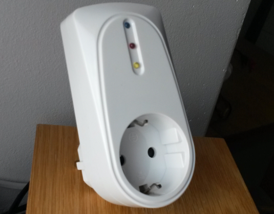
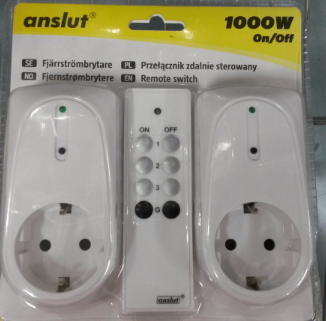
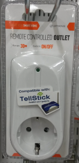
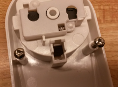
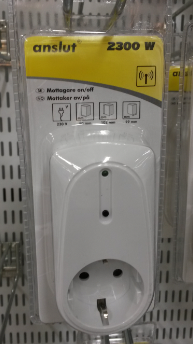
I went to a local shop and bought the cheapest 3-pack I could find, six months ago. I can't find it at that price (99SEK) any more, but the enclosure is (the most?) common, used by different brands and I guess very available in general. In worst case my new hardware of this project could be redesigned to fit other enclosures.
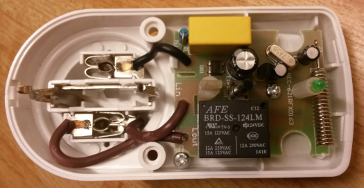
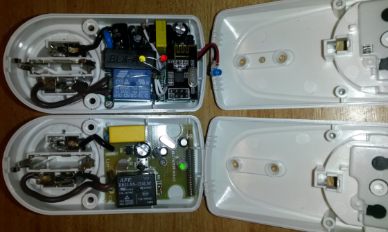
The internal parts of the original product is like every other of these: Xcap-rectifier-filter, relay, tiny uC with eeprom, radio circuit, etc. Note all the unused space inside the enclosure. Yum yum.
Since I don't have the right triangular shaped tool to release the two screws holding the case halves together, I replaced them as soon as I released them (with a normal flat headed screwdriver of the right size). I found that the screws included in the 10pcs Magnetic Door Switch Sensors make a perfect replacement for these.
The New Hardware
Here's my initial requirements. It's important to know that the objective of this first design was to (1) Be safe and (2) Collect info enough to assess reliability. It was not intended to be a final version.
- Standard 5x20mm glass fuse. Proven, high breaking capacity, replaceable and flexible (e.g. testing different values).
- Thermal fuse(s). Protecting from supply and/or relay overheating consequences.
- Ability to measure temperatures of liable internal overheaters individually.
- Creepage distances with safety margin and a general HV-LV as well as HP-LP separation.
- Heat resistant assembly with robust withstanding insulation between HV conductive parts.
- Standard relay, minimum 10A rated.
- Low high-power resistance.
- EMC (hard to test though)
- Basic MySensors and Arduino functionality, FTDI, ISP
- No new enclosure penetrations (keep it class II)
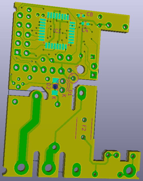
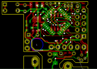
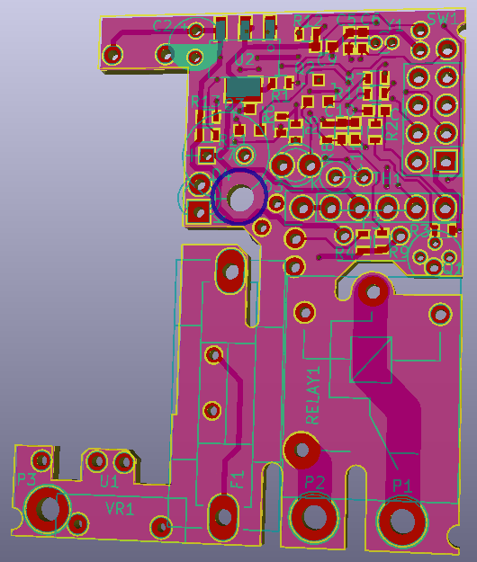
Running my Kicad, I came up with this:
Populated it looks like this:
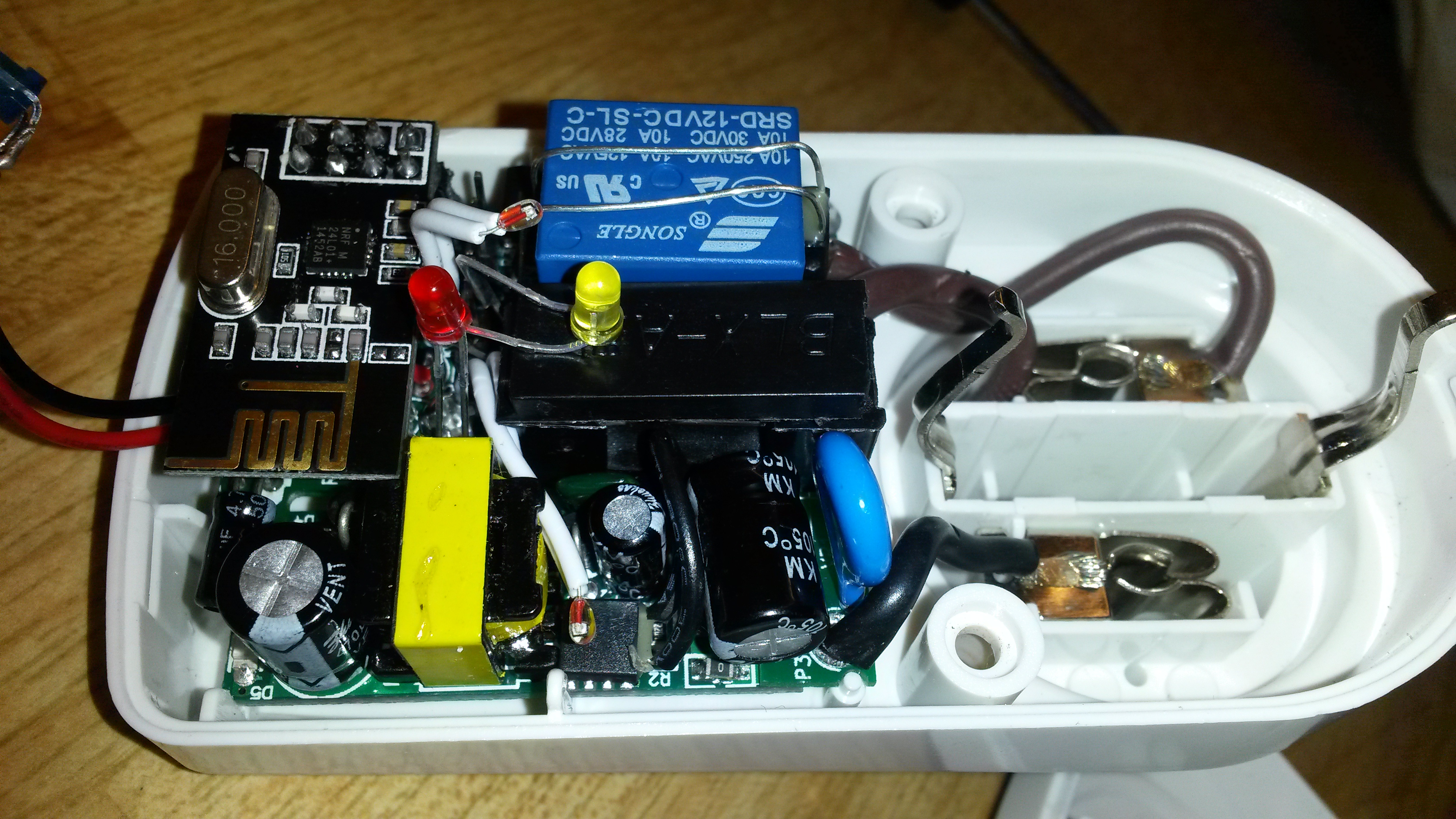
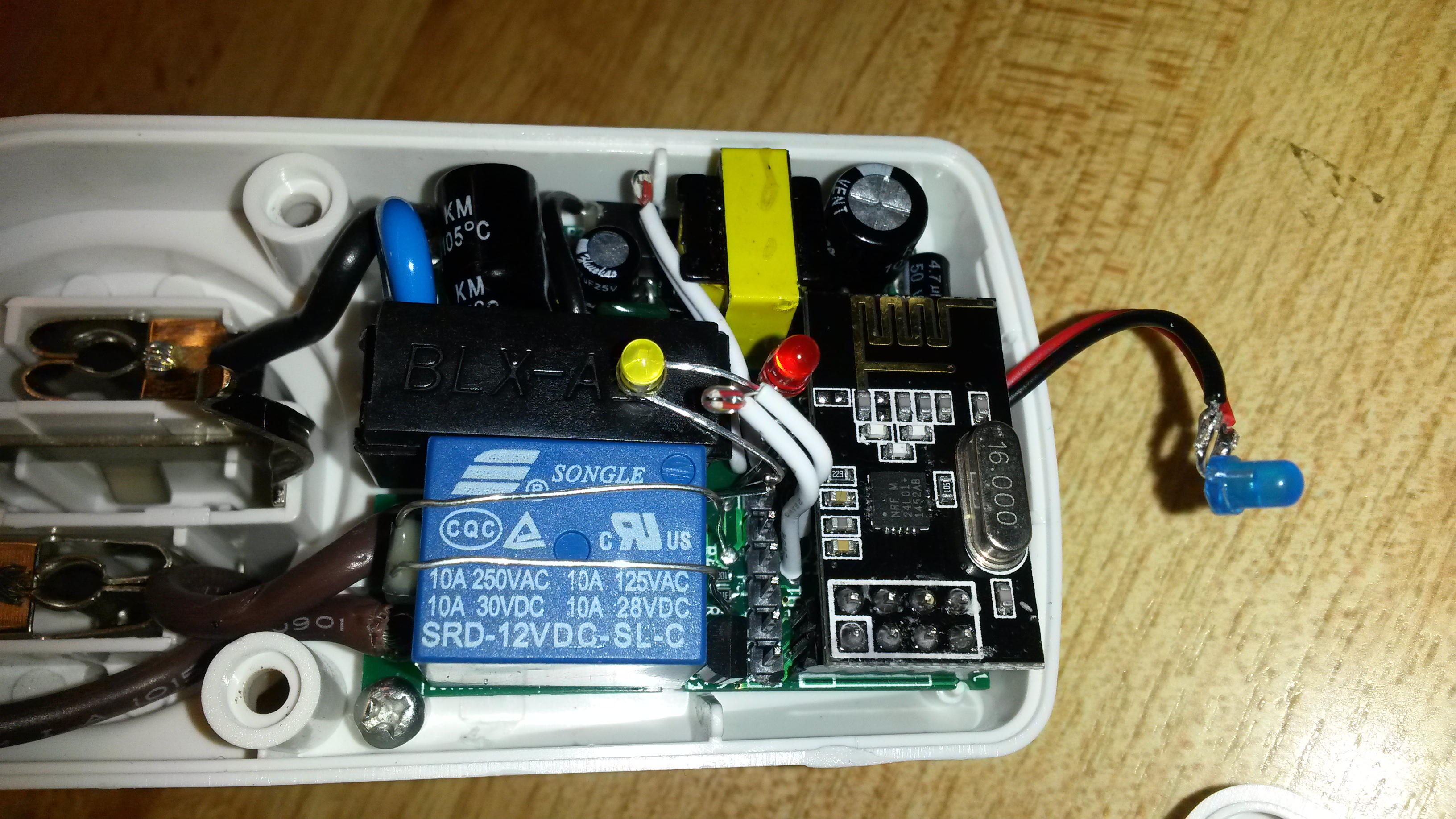
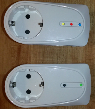
and with lid on it looks like this. As can be seen, instead of one button and one LED, I've put three LEDs.
Features of this prototype fulfil my overall requirements listed above (...I think. I really need a second opinion though.) To be more specific:
- Robust assembly where the supply module is attached to main PCB by multiple solder points and then main PCB are screwed in place at original fixation points.
- 5x20mm fuse in semi-covered fuse holder.
- Thermal fuse guarding the supply controller temperature
- Varistor 10D391K
- 12V switch mode supply with voltage-, current-, temperature protections and manageable EMI. (The supply module is the YS-12V400-B which I studied closer here)
- Songle 12V 10A relay
- Thermal fuse guarding the relay temperature
- Thermistors to monitor supply and relay temperatures
- Divider to monitor internal voltage and detect blown relay termo-fuse.
- As good creepage distance as possible and reasonable with respect to the supply input footprint
- Low resistance solder-filled high-power traces
- Higher resistance trace to internal power supply
- FTDI pins (only accessible by opening the enclosure.)
- ISP port (needs removal of the nRF24L01+ away from its socket).
- One yellow LED for passive status indication of relay state
- One blue and one red LED controlled from uC
- nRF antenna positioned near top and front of device (unfortunately also near the switch supply trafo, but it doesn't seem to cause any problem)
Kicad design files are shared, but there are a few minor fixes needed because of a few embarrassingly stupid but small errors. Gerbers not included due to this. See further below for furture development plans. Here's the board issues and necessary modifications:
- The +/- of the power module have been shifted. Solve by cutting traces and add jumper wires.
- The LED transistors (Q2 and Q3) have wrong footprint and must be placed 60' clockwise.
- The 5x20mm semi-closed fuse holder is placed 1-2mm too south and needs to be trimmed a little on the top edge to fit inside enclose. So put it with the lid hinge in the other end.
- The mounting hole in board middle is 0.5-1mm too small. The original screw fits, but not very nicely. There're also some value adjustments needed:
- Fuse value (0.1A) is much too low. Instead I'd recommend a 0.3-0.5A fast fuse.
- The blue and yellow LEDs are a bit to bright. Increase R4 and R11 some to fix that.
A warning to all beginners: This project requires a lot of skilled soldering. There are size 0603 SMD parts mixed with bigger parts and if you don't follow a plan for assembling and then test it step-by-step as you build, you'll probably never get it to work in the end. I haven't written an exact build order, but of course small SMDs must be soldered early for practical reasons. I think a good order to build and test is something like:
- SMDs
- nRF socket (to program uC bootloader via ISP, don't forget the 9th (Reset) pin. I use the standard Arduino Pro Mini 8MHz bootloader.)
- Avr-FTDI (test with Arduino IDE serial monitor)
- nRF
- 12V
- LEDs and thermistors
- Relay and relay control parts
- Thermal fuses (the one to the supply must soldered, before the glass fuse holder, to the board bottom side. Then folded up between supply module and board.)
- 5x20 glass fuse holder and supply module (YS-12V400-B or HX-12V400)
- Attach (solder) to the three line cables. (Double check to get it right.)
The legs of the thermistors and the thermal fuse to the supply must be insulated. Find some suitable wire, strip it off and pull the insulation on to the new parts.
And of course: Never ever do anything with 230V connected! Use 12V battery for testing the low voltage sections and functions, and test the high voltage and supply sections separately. I like to use battery instead of 12V supply to avoid risk of ground loop when powering 3.3V through FTDI (from my laptop) at the same time.
The Sketch
The sketch is aimed at testing and utilizes all the supported on-board hardware and tests LEDs, relay and status parameter conditions at start-up. Status conditions are monitored at start-up as well as during runtime. Errors and warnings are distinguished, processed and indicated through LED, coded controller messages and debug prints. Internal temperatures and voltage levels are measured every 1-3s (just my suggested set option) and reported at some optional interval to the controller. The error handling needs some improvement I think. E.g. there's sometimes a "low voltage error" when disconnecting the device from mains. Alarm (warning) and halt (error) levels need trimming and some hysteresis and "cooling-off delays". I know there's a lot of repeated code, few comments and probably other horrible software practices. Please disregard. It was quickly done and coding isn't my favourite part of this cooking. Thermistor calibration is done on a typical device, not every individual (e.g. this one). Accuracy seems to be good enough anyway, +/-3'C. (OT: If I some day automate my calibration process (off-line non-linear least mean square curve-fitting), it could be done for every node.)
Testing
Start-up inrush current values are presented in the supply review thread.
Current measurements at 239V AC: The succeeding "load" inrush current peaks at 15-20mA(rms) for <1s (just by looking at my Fluke). Then a few seconds at 8mA to finally settle at 6.5mA. With pulled relay this is 13.5mA at startup and then settled at 11mA. It means 1.5W power consumption at stand-by and 2.6W when relay is on. Ok, I think. Still in the very low load region of the supply load table), which is good according to my EMI guesses/theories in that thread.
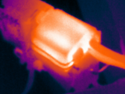
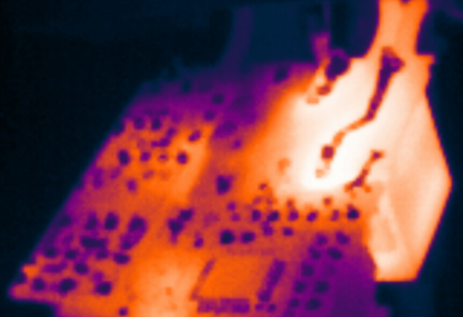
Load and Temperature: To be able to shoot the thermal images it's necessary to run with open enclosure. In theory, all temperatures will be higher after time in a sealed enclosure. It's anyway good the see how much different parts heat up compared to each other, and during which conditions.
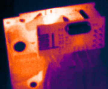
First image from one hour at idle. Highest temps measured to be the supply uC and rectifier diode and the AMS1117. All 35-38'C maximum. The supply uC heat isn't visible due the thermal fuse on top. Thermal fuses are not (yet) directly attached with thermal paste or glue, but it's on the to-do list.
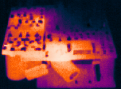
Next to the relay. A couple of minutes toggling the relay on-off at 0.5Hz with a 11A (at 239V) resistive load will look like this image below. Max temp ~40'C. It's easy to see that the heat is concentrated to the south part of the relay and that the thermal fuse is placed very good. I guess an inductive load would be much worse, but I haven't yet got to it.
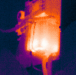
Next two relay images show status after several minutes at a continuous 11A load. Max temp 55'C. This test generated much more heat than the toggle test. Also I think maybe the bottom image illustrates the importance of solder-reinforce the high power traces - there's a lot more heat where I scrimped with solder paste.
Here are the controller (Fhem) registrations from the temperature sensors during a test. Plug connected to outlet at 14:00, 11A load is switched on at 14:10 and switched off at 14:17.
Future Development
This project was a little more time consuming than I'd planned. There were few aspects to it and I really want to reassure myself that it was a feasible (safe) design. So it's still far from finished. But working. What I need to do next is:
- Clear the board issues above.
- Attach thermal fuses with thermal paste or glue.
- Max inductive load endurance test.
- Build a few more prototypes.
- Install in "safe places" and set proper controller alarm and measures (back-up switch?).
- More operation time and collect more statistics.
Version 2.0
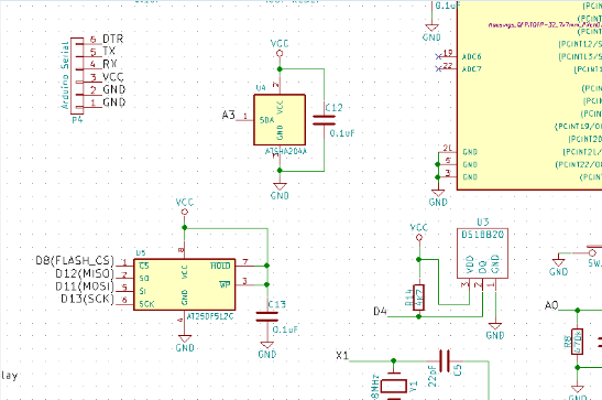
Along with this board version 1.0 I've also designed a 2.0. Is intended to be more of a production version rather than for testing. It has:
- One DS18B20 instead of thermistors (thermal fuses are kept of course)
- ATSHA204 (for signing purpose)
- External flash (for dual FTDI and OTA bootloader)
Unfortunately I got stuck quite early at the testing with the 2.0 prototype version. And I don't know when I'll have time to pick it up. If anyone is interested I think it's better to share that design in a separate thread and develop as a fork to the progress of this "test" version 1.0.
That's it. Unfortunately I can't estimate any schedule for finish this project, but I've had great fun wiith it so far. Hope you'll enjoy too.
